- 您现在的位置:买卖IC网 > Sheet目录342 > MCZ33285EFR2 (Freescale Semiconductor)IC TMOS DRIVER DUAL HISIDE 8SOIC
FUNCTIONAL DESCRIPTION
INTRODUCTION
FUNCTIONAL DESCRIPTION
INTRODUCTION
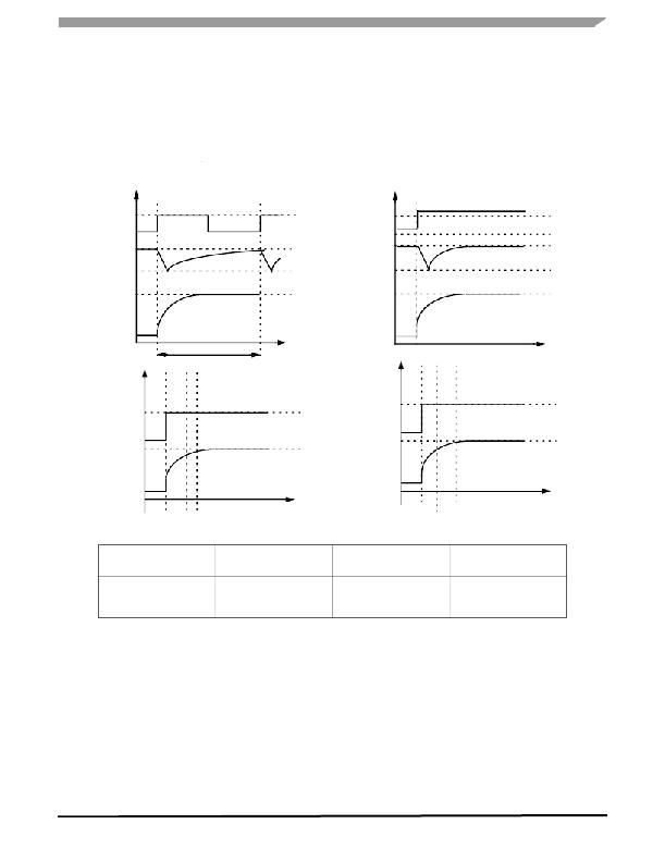
The power FETs are turned ON by charging their gate
capacities with a current flowing out of pins OUT1 and OUT2.
During PWM, the values of table below are guaranteed. They
are measured with 8.0 nF on OUT1 and 16 nF on OUT2. Test
condition V IN : ramp 0 V ≤ 2.5 V or 2.5 V ≤ 5.0 V.
IN
5.0 V
2.5 V
V CCP
IN
THRIN2
THRIN1
V OUT1
V VCC + 7.0
V OUT2
20 ms
V OUT2
5.0 V
IN
2.5 V
0V
IN
2.5 V
V OUT2MAX
V OUT1MAX
V OUT2
V OUT1
0V
0
t ON1 t ON2
t ON3
0V
0
t ON1
t ON3
t ON2
VOLTAGE V VCC
7.0 V < V VCC < 10 V
10 V < V VCC < 20 V
20 V < V VCC < 40 V
MINIMUM V OUT 1, OUT2
AFTER T ON1 = 100 μ SEC
V VCC - 0.7 V
V VCC - 0.7 V
V VCC - 0.7 V
MINIMUM V OUT 1,OUT2
AFTER T ON2 = 1.0 μ SEC
V VCC + 5.95 V
V VCC + 9.35 V
MINIMUM V OUT 1,OUT2
AFTER T ON3 = 1.5 μ SEC
V VCC + 7.0 V
V VCC + 11 V
Figure 4. Turn On Behavior
Turn Off Characteristics
The output voltages at OUT1 and OUT2 are limited by
controlling the current sources I ON1 , I ON2 to avoid current
flowing through the external or the internal zener diode.
When voltage power supply plus threshold voltage
(V CC + V TH ) is reached, the current sources are turned OFF.
? Threshold V TH1 for OUT1 output voltage control is
7.0 V < V TH1 < V Z
? Threshold V TH2 for OUT2 output voltage control is
7.0 V < V TH2 < 15 V
The power FETs on OUT1 and OUT2 are turned OFF by
discharging the gate capacity with the constant discharge
current I OUTOFF .
? Discharge current I OUTxOFF is I OUTxOFF = 110 μ A
condition: V OUT x > 0.5 V ( V IN < V THRxIN )
? Test conditions for switching OFF the power FETs:
1. IN open
2. Stages disabled via pin IN
3. Stage OUT1 disabled by an over current error
33285
Analog Integrated Circuit Device Data
Freescale Semiconductor
7
发布紧急采购,3分钟左右您将得到回复。
相关PDF资料
MCZ33927EK
IC FET PRE-DRIVER 3PH 54-SOIC
MCZ33937EKR2
IC PRE-DRIVER 3PHASE 54-SOIC
MDN2BL3GRAS
MOTOR BRUSHED DC 2V 2753RPM
MDN3BL3CSAS
MOTOR BRUSHED DC 2V 1458RPM
MIC2287-34YML TR
IC LED DRIVER WHITE BCKLGT 8-MLF
MIC2289C-34YD6 TR
IC LED DRIVR WHITE BCKLGT TSOT-6
MIC2291YD5 TR
IC LED DRIVER PHOTO FLASH TSOT-5
MIC2293-15YML TR
IC LED DRIVER WHITE BCKLGT 8-MLF
相关代理商/技术参数
MCZ33287EG
功能描述:功率驱动器IC CONTACT MONITOR DUAL LO RoHS:否 制造商:Micrel 产品:MOSFET Gate Drivers 类型:Low Cost High or Low Side MOSFET Driver 上升时间: 下降时间: 电源电压-最大:30 V 电源电压-最小:2.75 V 电源电流: 最大功率耗散: 最大工作温度:+ 85 C 安装风格:SMD/SMT 封装 / 箱体:SOIC-8 封装:Tube
MCZ33287EGR2
功能描述:功率驱动器IC CONTACT MONITOR DUAL LO RoHS:否 制造商:Micrel 产品:MOSFET Gate Drivers 类型:Low Cost High or Low Side MOSFET Driver 上升时间: 下降时间: 电源电压-最大:30 V 电源电压-最小:2.75 V 电源电流: 最大功率耗散: 最大工作温度:+ 85 C 安装风格:SMD/SMT 封装 / 箱体:SOIC-8 封装:Tube
MCZ33287R2
制造商:FREESCALE 制造商全称:Freescale Semiconductor, Inc 功能描述:Contact Monitoring and Dual Low-Side Protected Driver
MCZ33290EF
功能描述:外围驱动器与原件 - PCI ISO LINK RoHS:否 制造商:PLX Technology 工作电源电压: 最大工作温度: 安装风格:SMD/SMT 封装 / 箱体:FCBGA-1156 封装:Tray
MCZ33290EF/R2
制造商:FREESCALE 制造商全称:Freescale Semiconductor, Inc 功能描述:ISO K Line Serial Link Interface
MCZ33290EFR2
功能描述:外围驱动器与原件 - PCI ISO LINK RoHS:否 制造商:PLX Technology 工作电源电压: 最大工作温度: 安装风格:SMD/SMT 封装 / 箱体:FCBGA-1156 封装:Tray
MCZ33291EG
功能描述:电源开关 IC - 配电 BASIC OCTAL SERIAL SW RoHS:否 制造商:Exar 输出端数量:1 开启电阻(最大值):85 mOhms 开启时间(最大值):400 us 关闭时间(最大值):20 us 工作电源电压:3.2 V to 6.5 V 电源电流(最大值): 最大工作温度:+ 85 C 安装风格:SMD/SMT 封装 / 箱体:SOT-23-5
MCZ33291EGR2
功能描述:电源开关 IC - 配电 BASIC OCTAL SERIAL SW RoHS:否 制造商:Exar 输出端数量:1 开启电阻(最大值):85 mOhms 开启时间(最大值):400 us 关闭时间(最大值):20 us 工作电源电压:3.2 V to 6.5 V 电源电流(最大值): 最大工作温度:+ 85 C 安装风格:SMD/SMT 封装 / 箱体:SOT-23-5
